Table of Contents
DRAM Basics DDR DDR4 DDR4X LPDDR LPDDR4X
DDR4 SDRAM - Understanding the Basics
DDR4 SDRAM - Initialization, Training and Calibration
DDR4 Board Validation Simulation
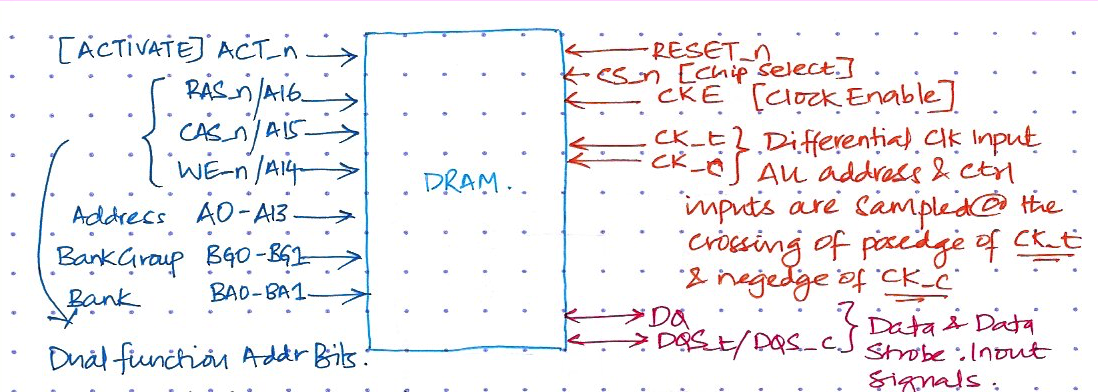
Top Level
| Symbol | Type | Function |
|---|---|---|
| RESET_n | Input | DRAM is active only when this signal is HIGH |
| CS_n | Input | The memory looks at all the other inputs only if this is LOW. |
| CKE | Input | Clock Enable. HIGH activates internal clock signals and device input buffers and output drivers. |
| CK_t/CK_c | Input | Differential clock inputs. All address & control signals are sampled at the crossing of posedge of CK_t & negedge of CK_n. |
| DQ/DQS | In/Out | Data Bus & Data Strobe. This is how data is written in and read out. The strobe is essentially a data valid flag. |
| RAS_n/A16, CAS_n/A15, WE_n/A14 | Input | These are dual function inputs. When ACT_n & CS_n are LOW, these are interpreted as Row Address Bits. When ACT_n is HIGH, these are interpreted as command pins to indicate READ, WRITE or other commands. |
| ACT_n | Input | Activate command input |
| BG0-1, BA0-1 | Input | Bank Group, Bank Address |
| A0-13 | Input | Address inputs |
BankGroup, Bank, Row, Column
DRAM Sizing & Addressing
DRAMs come in standard sizes and this is specified in the JEDEC spec. JEDEC is the standards committee that decides the design and roadmap of DDR memories. This is from section 2.7 of the DDR4 JEDEC specification (JESD79-4B).
DRAM Page Size
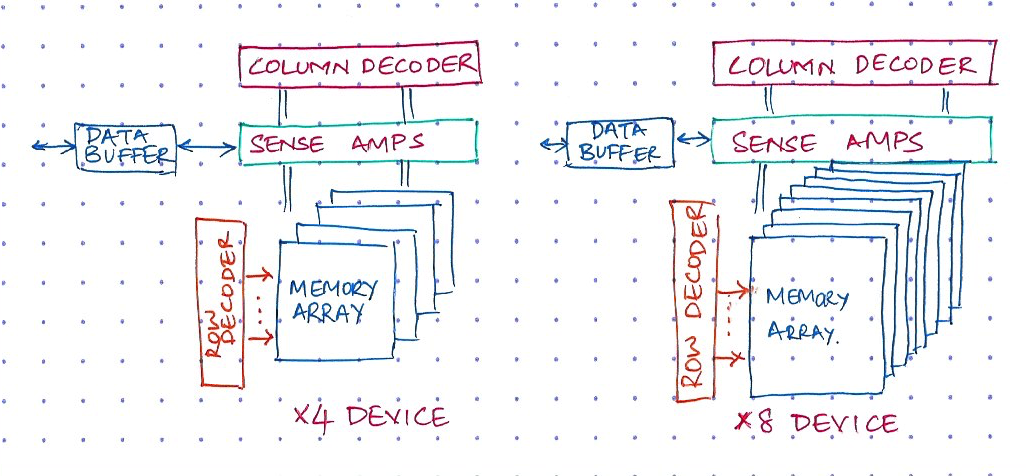
In the table above, there's a mention of Page Size. Page size is essentially the number of bits per row. Or put it another way, it is the number of bits loaded into the Sense Amps when a row is activated. Since the column address is 10 bits wide, there are 1K bit-lines per row. So, for a x4 device number of bits is 1K x 4 = 4K bits (or 512B). Similarly, for x8 device it is 1KB and for x16 it is 2KB per page.
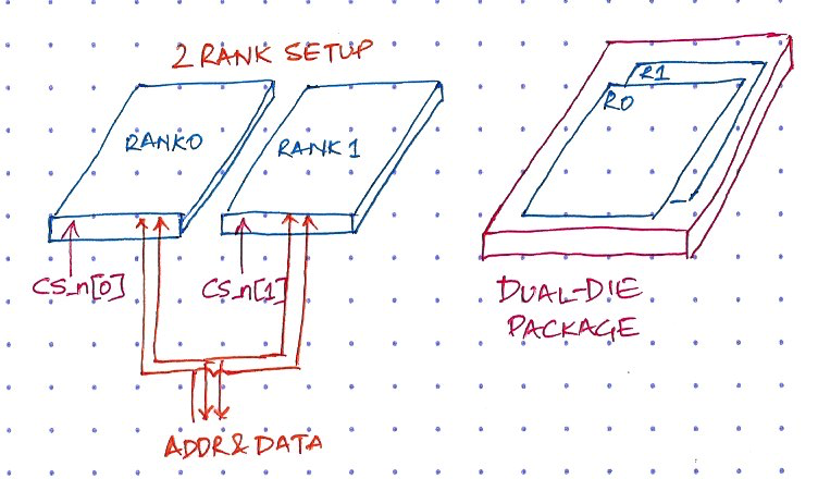
Rank (Depth Cascading)
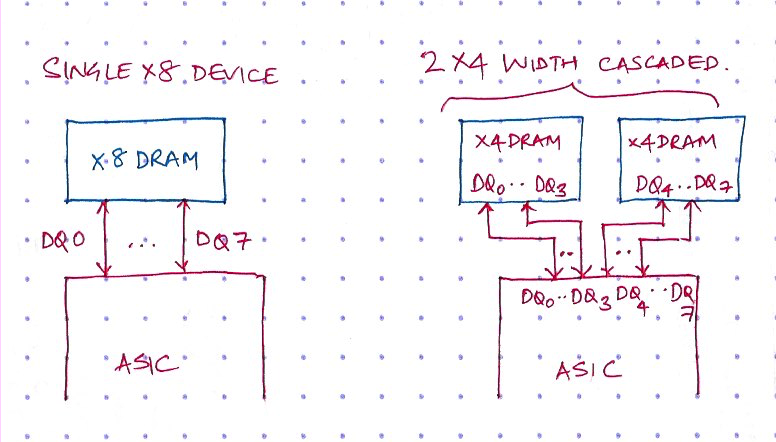
Width Cascading
Accessing Memory
Command Truth Table
I'm constantly referring to something called “commands” - ACTIVATE command, PRECHARGE command, READ command, WRITE command. But in the very first picture of this article, there is no “Command” input to the DRAM. So how are these commands issued?
Well, the DRAM interprets the ACT_n, RAS_n, CAS_n & WE_n inputs as commands based on the truth table below.
The table above is only a subset of commands you can issue to the DRAM. The entire DDR4 command truth table is specified in section 4.1 of the JEDEC spec JESD79-4B.
Read
Write
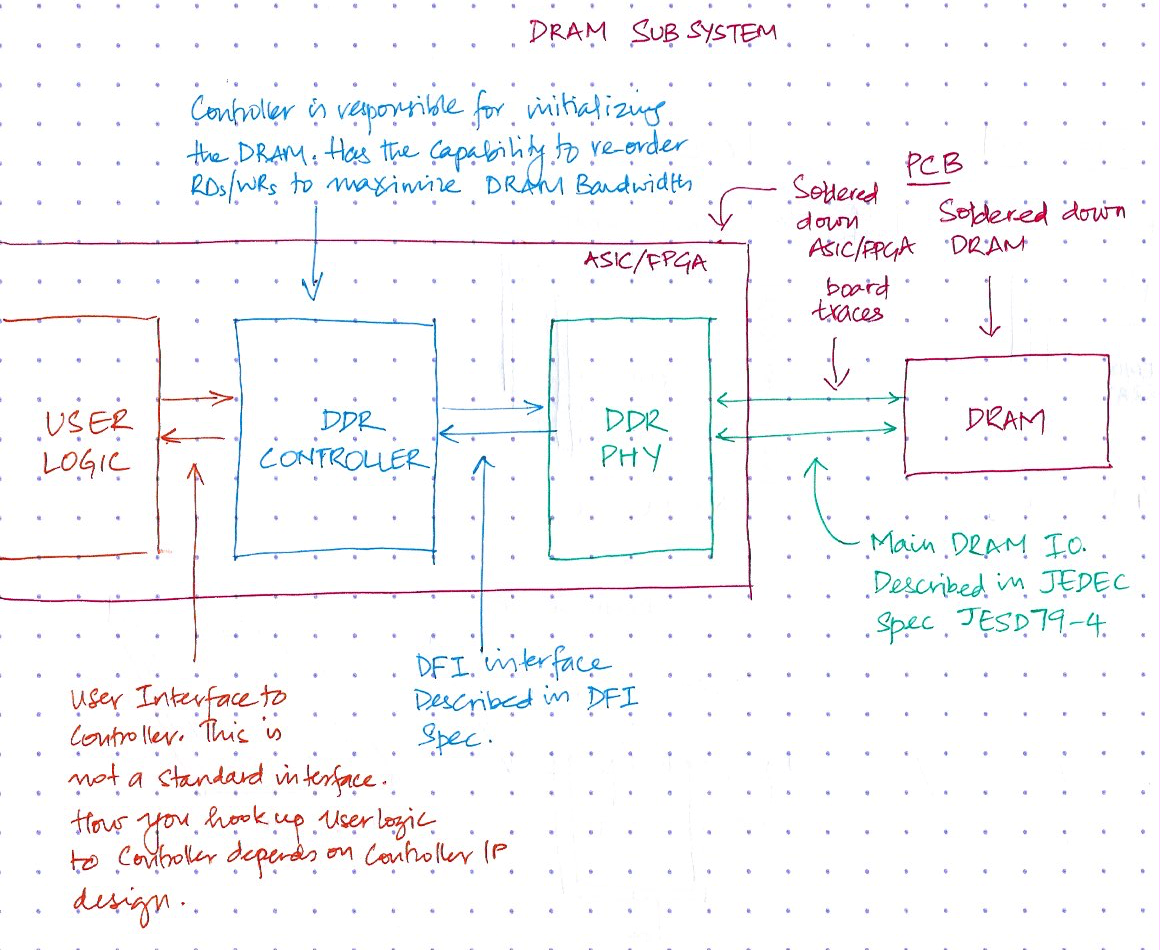
DRAM sub-system
Now that we've had a sufficiently long discussion about the DRAM, it is time to talk about what the ASIC or FPGA needs in-order to talk to the DRAM. This is called the DRAM sub-system and it's made up of 3 components:
- The DRAM memory itself, which comprises of everything described above
- A DDR PHY
- A DDR Controller
In a Nutshell
Let's wrap this up
The DRAM is organized as Bank Groups, Bank, Row & Columns The address issued by the user is called Logical Address and it is converted to a Physical Address by the DRAM controller, before it presented to the memory DDR4 DRAMs are classified as x4, x8 or x16 based on the width of the DQ data bus You can depth cascade or width cascade DRAMs to achieve the required size Read and write operations are a 2-step process. 1st step activates a row, 2nd step reads or write to the memory. The DRAM sub system comprises of the memory, a PHY layer and a controller
