This is an old revision of the document!
DRAM Basics
High Level
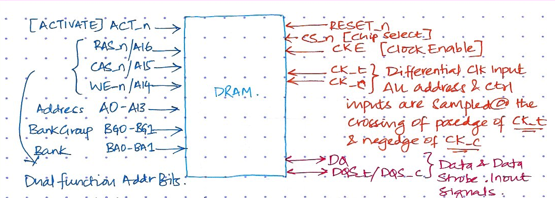
| Symbol | Type | Function |
|---|---|---|
| RESET_n | Input | DRAM is active only when this signal is HIGH |
| CS_n | Input | The memory looks at all the other inputs only if this is LOW. |
| CKE | Input | Clock Enable. HIGH activates internal clock signals and device input buffers and output drivers. |
| CK_t/CK_c | Input | Differential clock inputs. All address & control signals are sampled at the crossing of posedge of CK_t & negedge of CK_n. |
| DQ/DQS | In/Out | Data Bus & Data Strobe. This is how data is written in and read out. The strobe is essentially a data valid flag. |
| RAS_n/A16, CAS_n/A15, WE_n/A14 | Input | These are dual function inputs. When ACT_n & CS_n are LOW, these are interpreted as Row Address Bits. When ACT_n is HIGH, these are interpreted as command pins to indicate READ, WRITE or other commands. |
| ACT_n | Input | Activate command input |
| BG0-1, BA0-1 | Input | Bank Group, Bank Address |
| A0-13 | Input | Address inputs |
